See the Difference, Atom by Atom
Real MEP reconstructions from our founding team's published and collaborative research — the same engine that powers our software and services.
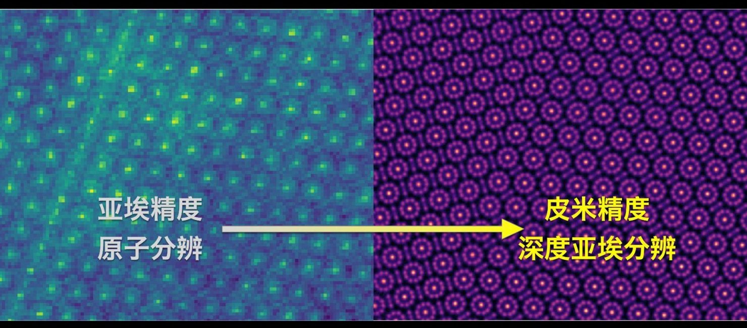
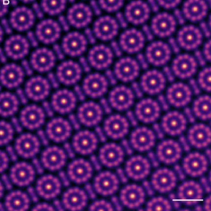
Point Defects in B₄C
Individual point defects resolved atom by atom — C-B-C vs C-V-C chain configurations distinguished directly in the reconstruction, validated against multislice simulation.
S. Ning et al., Science Advances 11, eadr4648 (2025)
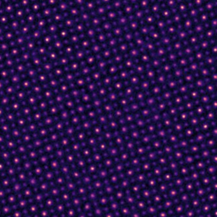
Twisted SrTiO₃ Bilayer
Layer-resolved reconstruction of a 5 nm + 5 nm twisted stack: upper and lower lattices and the moiré interface separated along the beam direction — impossible with projection imaging.
Founding team research, Univ. of Tokyo
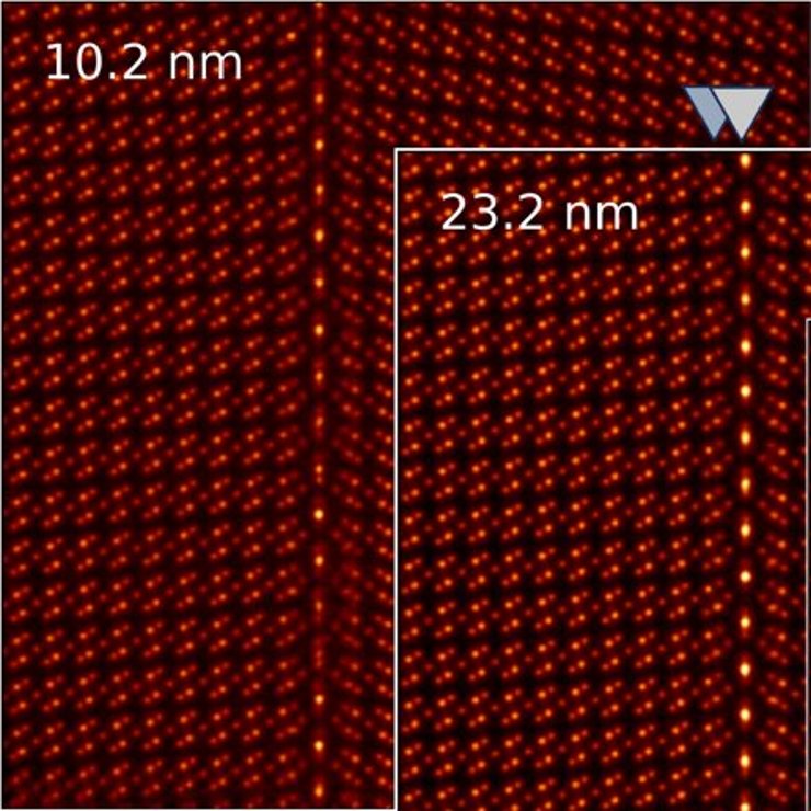
Depth-Sectioned Grain Boundary
Lu-doped Al₂O₃ Σ13 grain boundary imaged slice by slice from 0 to 36 nm depth — revealing a lateral boundary shift invisible to any 2D technique.
Founding team research, Univ. of Tokyo
Results shown are from peer-reviewed publications and collaborative research by our founding team.